Making electrical connections between various elements in a circuit is at the heart of electronics. There are many ways to do this, such as soldering wires to pins attached to a breadboard.
This can be very tedious. It also gets exponentially more difficult and messy when dealing with more complicated circuits. The next step to prototyping circuits is using software to make a schematic and layout a footprint that can be made on a PCB. This can be done relatively faster with the following etching technique.
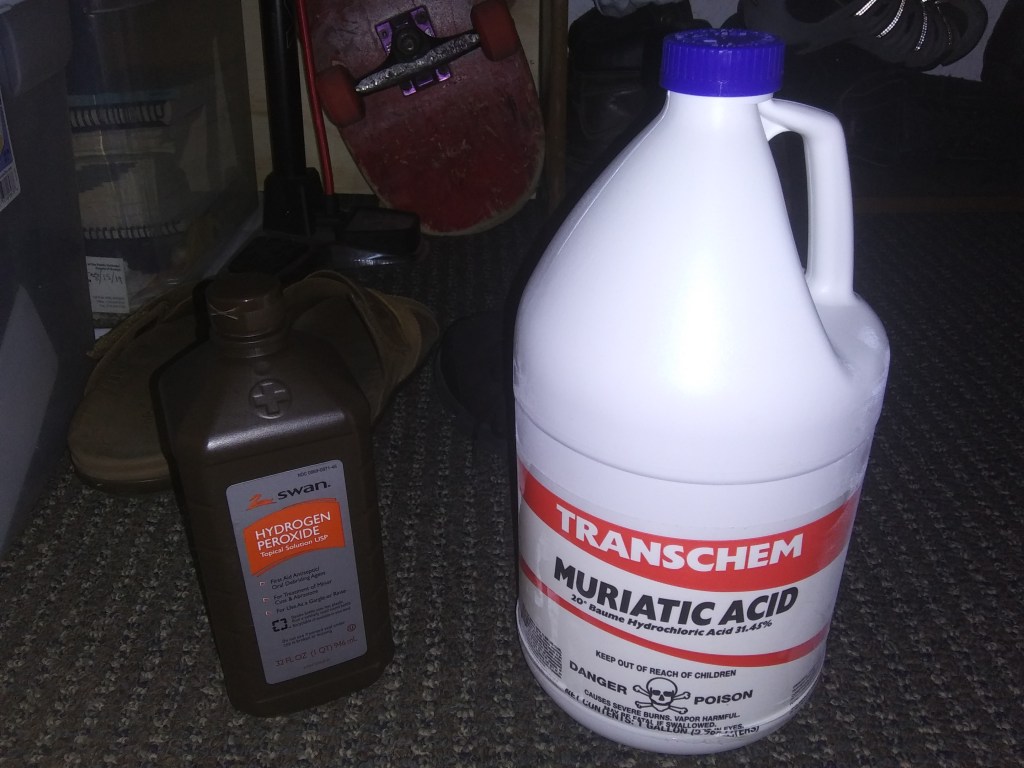
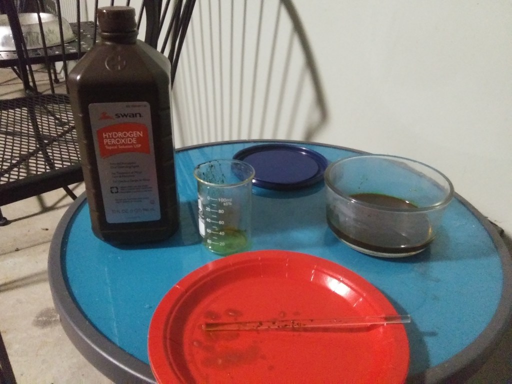
The first thing I did was prepare some etching solution. Their are a variety of solutions that people use, the most popular of which that I decided to make is Ferric Chloride. By first mixing 50mL of Muriatic Acid (found at Ace Hardware) with a spoon of Iron filings (bought off Amazon), periodically stirring and letting settle/react for a few hours. After slowly adding 50 mL of Hydrogen Peroxide (found at CVS), I am left with enough Ferric Chloride to carry out several etchings.
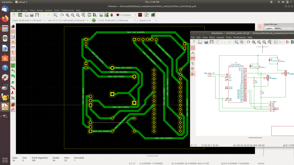
So, having etching acids was cool. The next part is designing the circuit. I like to use KiCAD. It is great, it is free, and it is an all in one bundle where you can create a schematic, test it with PSpice for functionality and comes with a PCB editor where you can customize component footprints and layouts. The software is all inclusive and created by our friends at CERN.
Once this is done you can output a Gerber file along with a drilling file to help with drilling holes for the pins. You have to print this with a laser printer. This is important because the laser printer uses toner. The next step requires toner to work. What we are going to do is transfer the circuit image onto a copper clad sheet. You can’t transfer dye based ink as is found in inkjet printers. We transfer the toner with heat by taping the laser printed image to our copper clad and running it through a laminator (oh yeah, printing on glossy photo paper is key). I modified my laminator by soldering a resistor in series with the internal thermistor to make it even hotter, but not sure this was necessary. After rolling this through the laminator 10 times or so, I used running water to help peel the paper off. This was my result.
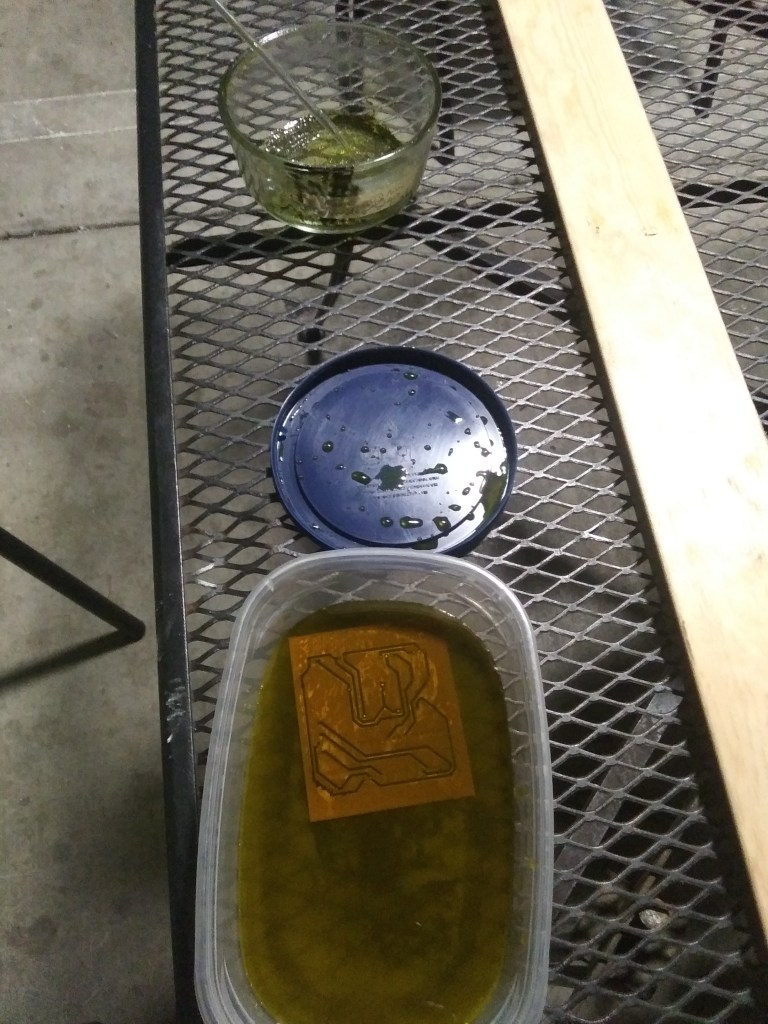
Finally, putting this into my etching cause all of the exposed copper to be dissolved leaving all of the copper protected by the toner. I ended up with a nice little circuit. After etching I cleaned the toner from the board using Acetone.
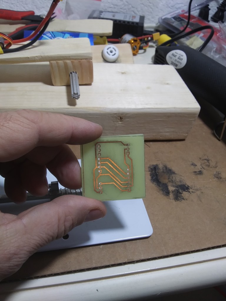
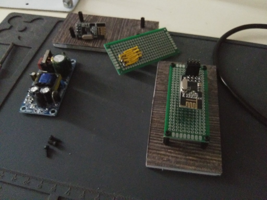
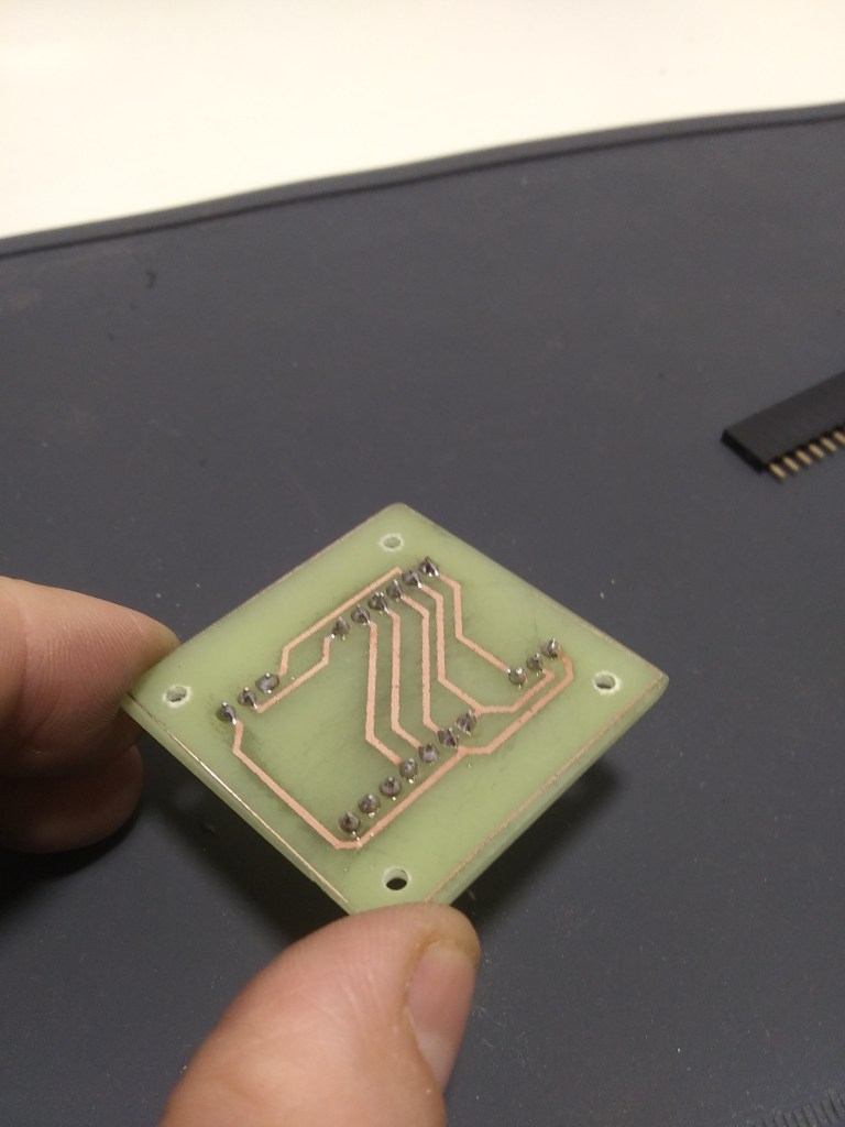
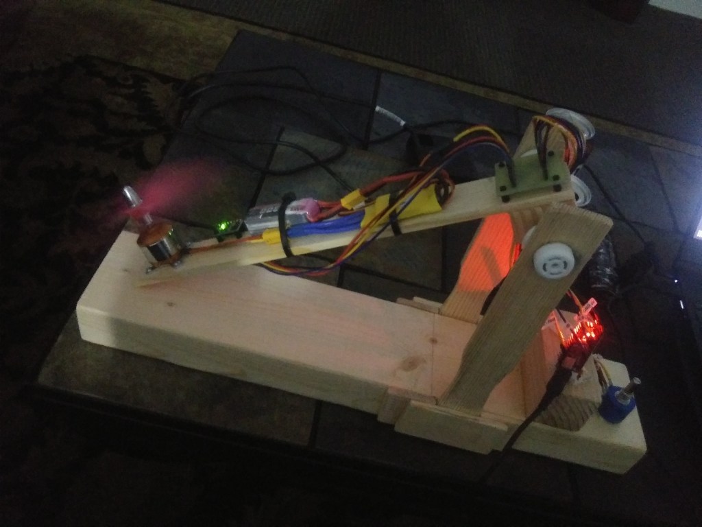
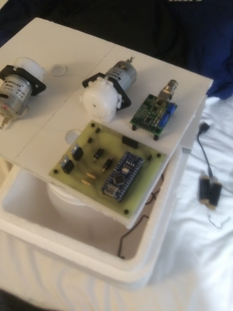
Having used a small jewler’s hand drill to make the holes, I proceeded to solder connectors for my cables, and had a much more organized way of dealing with the cabling and connections. This was my first, hand etched board, used to coordinate between gyroscope, Arduino Nano, Resistor Pot, and XPS motor controller.
My second one with the same fluid will be used to help control PH levels in a nutrition tank. This board has switching transistors and the Arduino Nano is placed directly on the board.
To make drilling quicker and easier I bought a dremel tool with a drill press stand. Looking forward to try making double sided board with via’s soon.